Flex & Rigid-Flex PCB Manufacturing Capability (2021) |
||||
|
Serial |
Item |
Flex PCB |
Rigid-Flex PCB |
|
|
1 |
Layers Counts |
1- 12 Layers |
2-16 Layers |
|
|
2 |
Material Type |
PI, PET, Kapton |
PI+FR-4 |
|
|
3 |
Material Brand |
SHENGYI, TAIFLEX, ITEQ, DuPont etc |
||
|
4 |
Stiffener Material Type |
FR-4, PI, PET, Steel, Al, Adhesive Tape |
||
|
5 |
Min Board Thickness |
1 Layer |
0.05mm(2mil) |
|
|
2 Layers |
0.10mm(4mil) |
0.20mm(8mil) |
||
|
6 |
Max Board dimension |
250*1000mm (9.84*39.37 inches) |
||
|
7 |
Min Trace Width / Trace Spacing |
Copper thickness: 0.5 oz |
0.05/0.05mm(2/2mil) |
|
|
Copper thickness: 0.5 oz-1oz |
0.075/0.075mm(3/3mil) |
|||
|
Copper thickness: 1oz |
0.10/0.10mm(4/4mil) |
|||
|
8 |
Min Hole Diameter (Mechanical drill) |
0.15mm(6mil) |
||
|
9 |
Min Hole Diameter (Laser drill) |
0.10mm(4mil) |
||
|
10 |
Min Annular Ring (Outer layers) |
1 Layer |
0.10mm(4mil) |
|
|
2 Layers |
0.10mm(4mil) |
|||
|
11 |
Min Annular Ring (Inner layers) |
≧ 4Layers |
0.10mm(4mil) |
|
|
Min Annular Ring (Outer layers) |
0.10mm(4mil) |
|||
|
12 |
Coverlay thickness |
12.5um, 25um, 50um |
||
|
13 |
Min Coverlay Opening |
0.40*0.40mm(16*16mil) |
||
|
14 |
Min Solder mask Opening |
0.15mm(6mil) |
||
|
15 |
Min Coverlay Bridge |
0.20mm(4mil) |
||
|
Min Solder mask Bridge |
0.13mm(5mil) |
|||
|
16 |
Via Type |
Through Hole, Blind, Buried |
||
|
17 |
Tolerance |
PTH Hole |
±0.075mm(±3mil) |
|
|
NPTH Hole |
±0.05mm(±2mil) |
|||
|
Outline |
±0.10mm(±4mil) |
|||
|
Outside edge to Circuit |
±0.10mm(±4mil) |
|||
|
18 |
Surface finished |
ENIG, OSP, Immersion Silver, Immersion Tin, Glod Plating, Gold Plating+ENIG, Gold Plating+OSP |
||
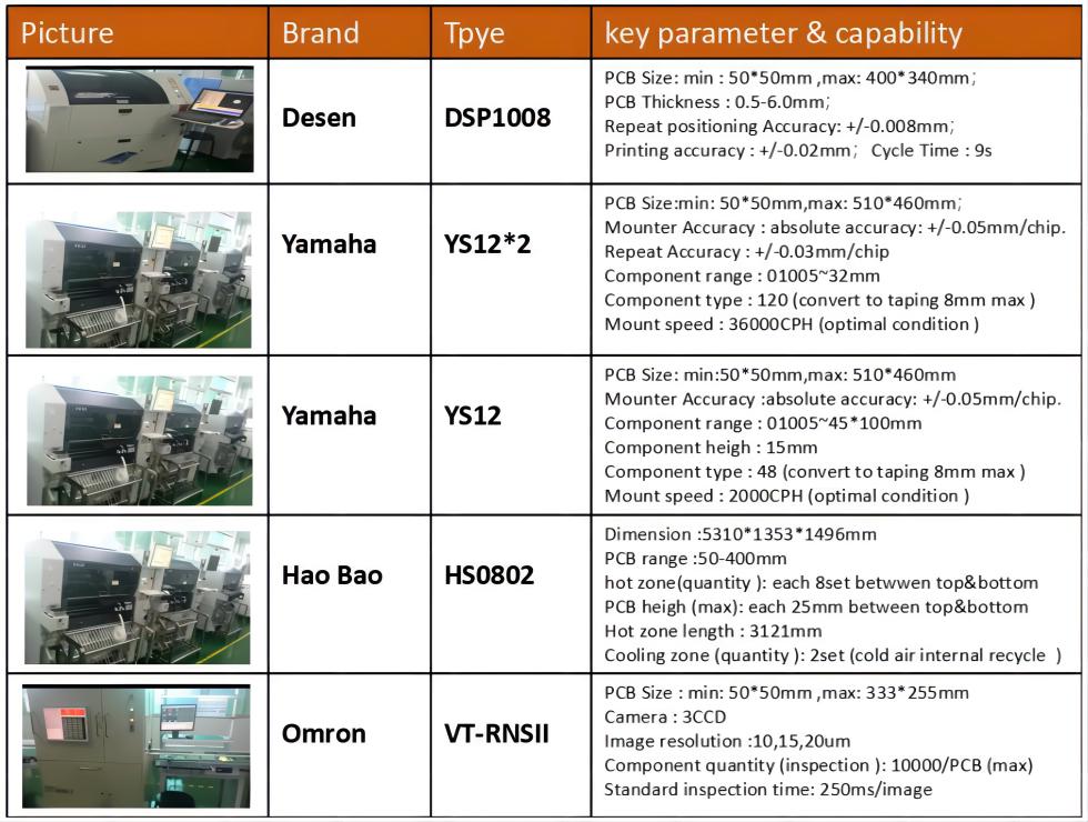
SMT Manufacturing Capability (2021) |
||||
|
Serial |
Item |
Manufacturing Capability in process |
Manufacturing Method |
|
|
1 |
Production size(Min/Max) |
50×50mm / 510×460mm |
|
|
|
2 |
Production board thickness |
0.20~6.00mm |
|
|
|
3 |
Printing solder paste |
Support method |
|
Magnetism fixture, Vacuo platform |
|
Clamping method |
|
Sticking up by vacuo, clamping on both sides ,flexible clamping with sheet, flexible clamping with thick board |
||
|
Cleaning Method of printing solder paste |
|
Dry method+ wetting method+ Vacuo method |
||
|
Accuracy of printing |
±0.02mm |
|
||
|
4 |
SPI |
Repeated accuracy of volume |
<1% at 3σ |
|
|
5 |
Mounting component |
Components size |
0603(Option) L75mm Connector |
Online |
|
Pitch |
0.15mm |
|
||
|
Repeated accuracy of volume |
±0.01mm |
|
||
|
6 |
AOI |
FOV size |
61×45mm |
Online |
|
Test speed(mm²/Sec) |
9150 |
|
||
|
7 |
3D X-ray |
Shooting angle(degrees) |
0-45 degree |
Online |
|
|
||||
|
DIP Manufacturing Capability (2021) |
||||
|
1 |
All plug-in components are tested for errors, omissions and misplacement of components using AOI to strictly control the pass rate of DIP processing. |
|||
|
2 |
Experienced soldering hands with strict training can control welding speed and quality. |
|||
|
3 |
According to the production status of PCB Assembly, a temporary storage area with independent identification should be equipped around the pull wire, such as waiting for plug-in area, waiting for maintenance area, waiting for QC inspection area, defective product area, waiting for QA inspection area, etc., to avoid the appearance of mixed boards. |
|||
|
4 |
Strict IPQC and QA LOT sampling inspection standards to ensure the reliability of DIP processing. |
|||
|
DIP Manufacturing equipment is as follows: |
||||
|
1 |
DIP Production lines x 2 sets. |
|||
|
2 |
AOI Equipment (Used to check DIP): Check for defects in plug-in components and solder joints. |
|||
|
3 |
Wave soldering x 2 sets. |
|||
|
4 |
Rear weld pull wire x 36 station. |
|||
|
5 |
Board washing machine x 1 set |
|||
Key Equipment Parameter


