
Greathome has been engaged in Rigid-flex PCB board for many years, we have accumulated a lot of experience in optimizing design and manufacturing. Through understanding customers' needs and combining with product application scenarios, our experts and engineers will evaluate and discuss with you each customized product through DFM/DFT analysis. From design to manufacturing, we will give our most reasonable suggestions and solutions based on our experience for your reference and confirmation.
We will help you reduce the time of R&D and design verification, and better manufacture the best Rigid-flex PCB board for you, for each of your works, from sample to mass production.
If you are looking for a reliable Rigid-flex PCB board partner in China, please don’t hesitate to contact us.
What are the available Types for Rigid-flex PCBs?
Printed Board Type Performance requirements are established for the different types of rigid-flexible printed boards, classified as follows:
Rigid-Flex PCB (IPC-6013 type 4) Multilayer rigid and flexible material combinations containing three or more conductive layers with PTHs.
Rigid-Flex PCB (IPC-6013 type 5) Flexible or rigid-flex printed boards containing two or more conductive layers without PTHs.
Our current Rigid-Flex PCB manufacturing capability is up to 2-16 Layers.
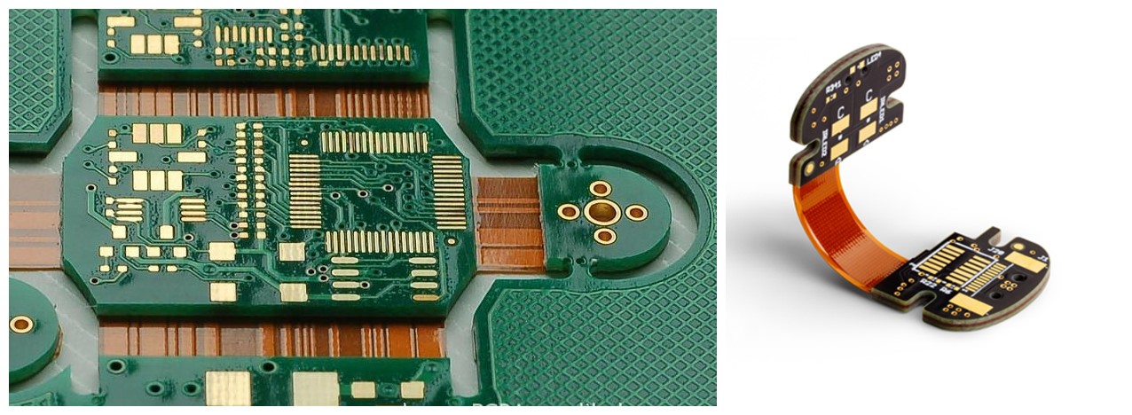
What is a Rigid-flex PCB board?
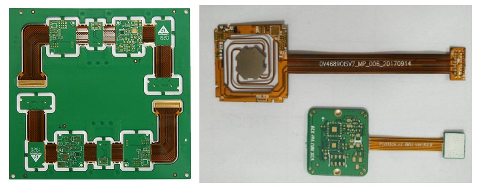
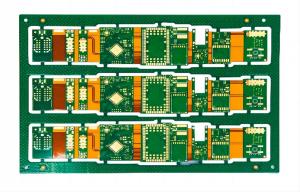
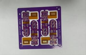
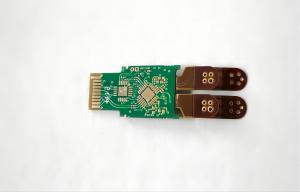
Rigid-flex PCB refers to flexible PCB board and Rigid PCB board, which are combined together according to relevant process requirements through Lamination and other processes to form circuit boards with FPC and Rigid PCB characteristics.
Most Rigid-flex PCB boards consist of several layers of flexible circuit substrate attached externally or internally to one or more Rigid PCB boards, depending on the design of the application. Flexible substrates are designed to be in a constant state of flexure and usually form flexible curves during manufacturing or installation. Rigid-Flex design is more challenging than typical Rigid PCB board environment design because these PCB boards are designed in 3D space, which also provides higher spatial efficiency.
Rigid-flex PCB board is a new type of printed circuit board which combines Rigid PCB durability and flexible PCB adaptability. Among all types of PCBS, Rigid- Flex combination is the most resistant to harsh application environment, so it is favored by manufacturers of industrial control, medical, military equipment etc.
Advantages of Rigid-flex PCB board
Rigid-flex PCB Board has both the characteristics of FPC and PCB, which can be used in products with special requirements, saving the internal space of products, reducing the volume of finished products and improving the performance of products.
Compared with Rigid PCB Board, the biggest advantage of Rigid-flex PCB Board is that it can be folded and assembled in a small area, which can effectively reduce the volume and weight of electronic products.
The biggest advantage of Rigid-flex PCB Board compared with flexible PCB Board is that it can provide more welding area, so it can meet the increasingly complex assembly and welding requirements of electronic components.
The advantages of Rigid-flex PCB board compared with Rigid PCB, such as:
1. Flexible, can be three-dimensional assembly, according to the space limit and change shape.
2. High and low temperature resistance, fire resistance.
3. Foldable, and does not affect signal transmission function.
4. It can prevent static interference.
5. Stable chemical change, safety and high reliability.
6. Beneficial to the design of related products, can reduce assembly time and errors, and improve the service life of related products.
7. Reduce the volume of the application products, greatly reduce the weight, increase the function and reduce the cost.
How to design a Rigid-flex PCB board?
Rigid-Flex PCB board is much more complicated than traditional PCB design, and there are many aspects to pay attention to in PCB circuit design. In particular, Rigid and Flexible transition areas, as well as related circuits, Via holes and other design aspects need to follow the requirements of the corresponding design rules.
1. Location of Via holes
In dynamic use, especially when FPC PCBS are often bent, via holes on FPC PCBS should be avoided as much as possible. These via holes can be easily damaged and cracked. However, NC drilling can be done in the Stiffener area on the Via hole, but it is also necessary to avoid the Stiffener area and maintain a safe distance along the Stiffener area. Therefore, when NC drilling in Rigid-Flex PCB Board design, we should avoid Rigid-flex combination area and keep a certain safe distance.
As shown below:
For the distance requirements of via hole and Rigid and flexible combination zones, the design rules should be followed as follows:
- keep a distance of at least 50mil. For high-reliability applications, keep a distance of at least 70mil.
- Most manufacturers will not accept the limit distance less than 30mil.
- Follow the same rule for Via hole on Flexible.
- This is the most important design rule for Rigid-flex PCB board.
2. Pads and Via holes design
Pads and via holes are maximized in accordance with electrical requirements. Smooth transition lines are used at the connection between pad and conductor to avoid right angles.
The individual pads should be added Anchors to enhance the support.
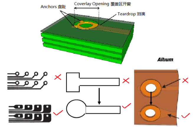
In Rigid-Flex PCB board design, Via hole or pad can be easily damaged, to reduce this risk need to follow the rules:
- Pad or Via hole should correspond to Coverlay opening layer, the bigger the better.
- Add Line Teardrops to Via holes’ conductor lines as much as possible to increase mechanical support.
- Add circuit pad anchors for reinforcement.
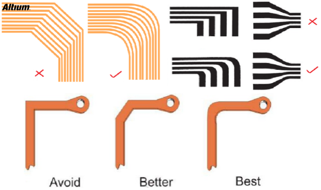
3. Circuits design
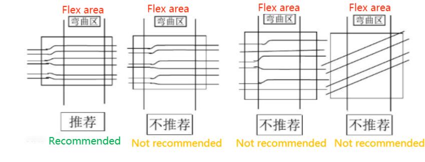
In the flexible zone (Flex), if there are circuits on different layers, try to avoid one circuit in the Top layer and the other circuit in the Bottom layer (the same path).
In this way, when Flexible bending, the force of the circuit on the upper and lower layers is inconsistent with that of the copper, which is easy to cause mechanical damage to the circuit. Instead, the circuit should be staggered and the paths should be cross neat rows.
Circuit design in the flexible zone (Flex) requires an arc line rather than an Angle line. Contrary to the advice of Rigid panels. In this way, the Flexible part of the circuit is protected from damage when bending. Sudden enlargement or decrease of a circuit should also be avoided, and arcs in the form of Line Teardrops should be used to connect the thick and thin circuits.
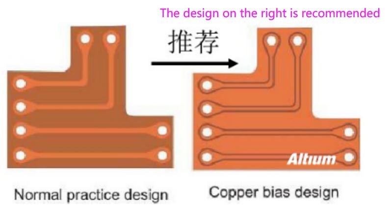
4. Laying copper design
In order to enhance the Flexible PCB Board's Flexible bending degree, it is best to make the laying copper design or network structure design for plane layer. However, for impedance control or other applications, the electrical quality of network structures is not satisfactory. Therefore, circuit designers need to choose the best way according to the design requirements, that is, using grid copper or copper.
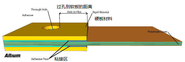
5. The distance between NC Drilling and copper
This distance refers to the distance between the hole and the copper, That is drill and copper distance. Flexible materials are different from Rigid materials, so it is difficult to deal with the holes and copper distance too close. The standard hole copper distance should be 10mil.
For Rigid and flexible combination zones, the two most important distances must not be ignored. One is called Drill to Copper, following a minimum standard of 10mil. The other is the Hole to Flex distance from the Hole to the outline of flexible PCB. 50mil is generally recommended.
6. Rigid and flexible combination zone design
In Rigid and flexible combination area, flexible is best designed to connect Rigid in the middle of stack. And the Via hole of Flexible in Rigid and Flexible combined zone is considered as buried hole. The Rigid and flexible combination zone needs to be noted as follows:
- The circuit trace should transition smoothly and the direction of the circuit trace should be perpendicular to the direction of bending.
- Conductor line should be evenly distributed throughout the bending zone.
- The width of the conductor line should be maximized throughout the bending zone.
- Rigid and flexible transition zone does not adopt PTH design as far as possible.
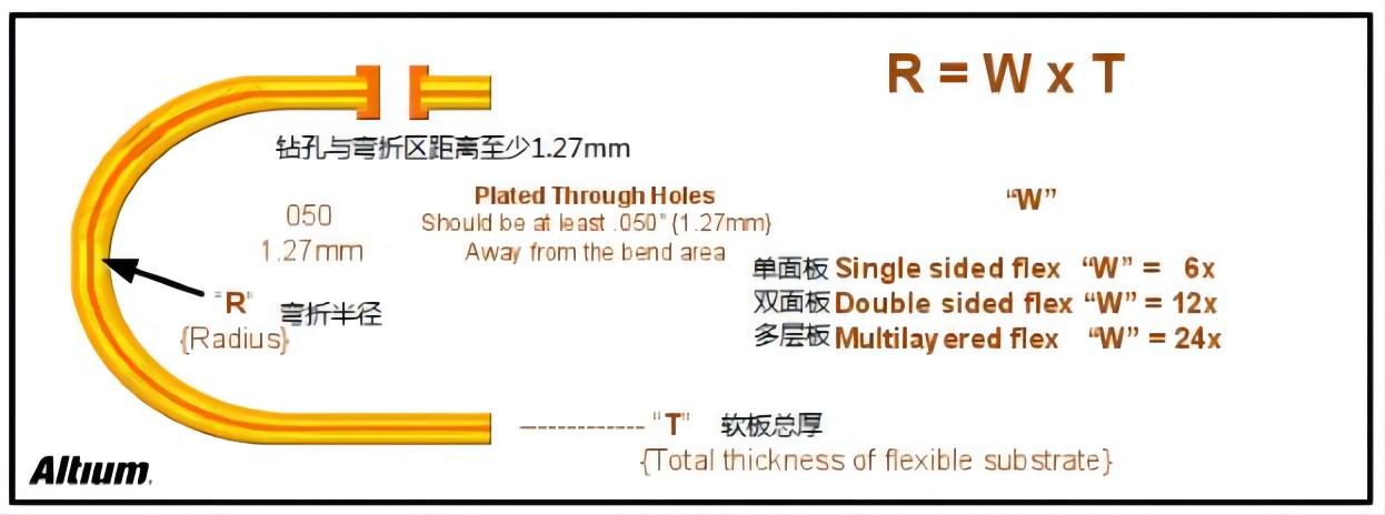
7. The bending radius of Rigid- Flex PCB Board’s bending area
Rigid-flex PCB Board's flexible bending area should be able to withstand 100,000 flexing without breaking, short circuit, performance degradation or unacceptable delamination. Flexing resistance, the use of special equipment, can also use the equivalent instrument determination, test samples should meet the requirements of the relevant technical specifications.In terms of design, bending radius should be as shown in the figure below for reference.
The bending radius design should be related to the thickness of the flexible board and the number of layers of the flexible board in the flexible bending area. A simple reference is R=WxT. T is the total thickness of the Flexible board. Single panel W is 6, double panel 12, and multilayer 24. Therefore, the minimum bending radius of single panel is 6 times the plate thickness, double panel is 12 times the plate thickness, and multi-layer panel is 24 times the plate thickness. All should not be less than 1.6mm.
In a word, for the Rigid- Flex PCB Board design, especially important is the Flexible circuit Board design. The design of Flexible Circuit board requires consideration of the substrate, paste layer, copper foil, cover layer, Stiffener and different materials, thicknesses and combinations of Stiffener surface treatment, as well as its performance. Such as peel strength, anti - flexure performance, chemical performance, working temperature, etc. Special consideration should be given to the assembly and specific application of the designed Flexible Circuit board. In this respect, specific design rules can refer to IPC standards: IPC-D-249 and IPC-2233.
Rigid-flex PCB Board applications
Rigid-flex PCB board provide a wide range of applications from smart devices to mobile phones and digital cameras. Rigid-flex PCB Board manufacturing has been increasingly used in medical devices such as pacemakers to reduce space and weight. The use of Rigid-flex PCB board has the same advantages and can be applied to intelligent control systems.
In consumer electronics applications, Rigid flex PCB Board not only maximizes space use and minimizes weight, but also greatly improves reliability, Then many requirements for welded joints and joint wires that are prone to connection problems (such as brittle/fragile) are eliminated. These are just some examples, but Rigid-flex PCB board can benefit almost all advanced electrical applications, including test equipment, tools and cars.
For example, common application areas are as follows:
- Camera, Video camera;
- CD-Rom, DVD;
- Hard drive, notebook computer;
- Telephone, Mobile phone;
- Printer, Fax machine;
- Television;
- Medical equipment;
- Automotive electronics;
- Aerospace and Military products, etc.