
Backdrill PCB Technology: A Key Enabler in 5G, Radar, and Server Applications
As the demand for high-speed and high-frequency electronics continues to grow, the importance of advanced PCB fabrication techniques like Backdrill is more critical than ever. From 5G communication systems to automotive radar and data center servers, signal integrity is the cornerstone of performance. Among the many high-frequency techniques available, Backdrill plays a crucial role in reducing signal reflection and ensuring impedance consistency.
In this blog, we’ll explore what Backdrill technology is, why it matters, and how it is applied in the most demanding applications today. We’ll also show how Greathome Group, a leading PCB/FPC/PCBA manufacturer, leverages this technology to deliver precise, high-performance electronic solutions across these critical industries.
What Is Backdrill in PCB Manufacturing?
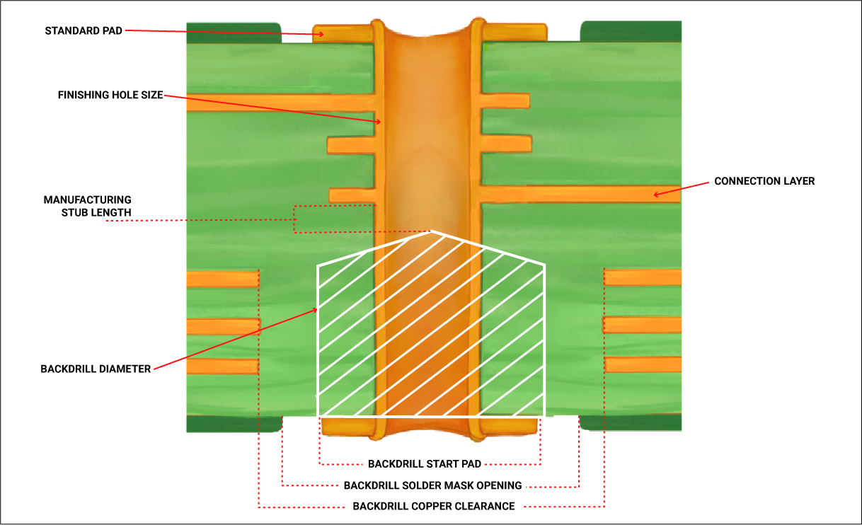
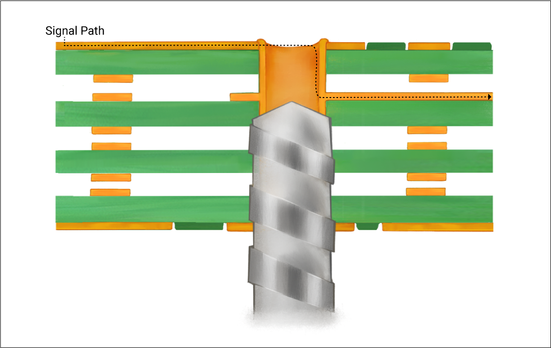
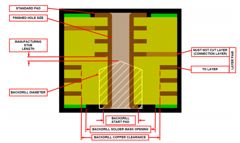
Backdrill is a mechanical drilling process used to remove the unused stub portion of a plated through-hole (PTH) via in a multi-layer PCB. When signals travel through vias that go beyond their intended layer connection, the leftover stub acts like an antenna, causing reflection, signal loss, and increased noise. This becomes a major issue in high-speed PCBs, especially when operating at 5GHz or higher.
By precisely "back drilling" the via to remove this stub, manufacturers ensure:
-
Minimal signal reflection
-
Improved impedance control
-
Reduced electromagnetic interference (EMI)
-
Lower bit error rates (BER)
Backdrill is typically done after the via plating process, using CNC or laser drilling machines with extremely tight depth tolerance control (±0.05mm or better).
Why Is Backdrill Essential in High-Frequency PCB Design?
In low-frequency designs, signal integrity may not suffer significantly from via stubs. However, in RF, microwave, or ultra-high-speed digital environments, stubs become an unacceptable bottleneck. Here’s why Backdrill is non-negotiable:
| Design Impact | Without Backdrill | With Backdrill |
|---|---|---|
| Signal Reflection | High | Minimal |
| Impedance Fluctuation | Unpredictable | Controlled |
| Crosstalk | Likely | Greatly Reduced |
| EMI | Elevated | Lowered |
| High-Speed Loss | Critical | Optimized |
Backdrill is often used in HDI PCBs, high-layer-count boards, and boards with critical signal paths like DDR6, PCIe Gen5/6, and mmWave antennas.
Application 1: Backdrill in 5G Communication Systems
5G and the Signal Integrity Challenge
With 5G operating in both sub-6GHz and mmWave bands (24–52GHz), signal integrity becomes extremely sensitive to design flaws. Every via stub acts as a reflection point that can distort MIMO signals, reduce bandwidth, or disrupt synchronization.
Where Backdrill Is Used in 5G PCBs:
-
Antenna modules: Reduces stub impact on RF feedlines
-
Beamforming arrays: Ensures uniform impedance across paths
-
Backplanes: Removes unnecessary via depth to maintain timing alignment
Greathome's Capability for 5G:
At Greathome Group, we provide:
-
Minimum drill diameter of 0.15mm
-
CNC-controlled depth tolerance within ±0.05mm
-
Verified via TDR testing, AOI, and X-ray for reliable signal consistency
-
Support for advanced 5G materials like Rogers RO4350B and high-Tg FR-4
We offer end-to-end support, from RF stack-up design to controlled impedance matching, enabling our customers to build next-gen 5G hardware with confidence.
Application 2: Backdrill in Automotive and Millimeter-Wave Radar Systems
Millimeter-Wave Radar PCB Design
Radar modules for ADAS (Advanced Driver Assistance Systems) and autonomous vehicles typically operate at 24GHz or 77GHz. At these frequencies, even a small via stub can act as a resonator, disrupting the antenna’s directional behavior and gain.
Benefits of Backdrill in Radar PCBs:
-
Cleaner antenna radiation patterns
-
Improved SNR (Signal-to-Noise Ratio)
-
Stable impedance in microstrip and stripline designs
-
Compliance with tight form factor and thermal constraints
Greathome’s advanced PCB fabrication supports:
-
Materials like Arlon 85N, Megtron 6, and low-Dk PTFE
-
Multi-pass backdrilling for radar front-end layers
-
Layer registration accuracy for mmWave stack-ups
-
AOI and TDR testing to verify radar channel consistency
Application 3: Backdrill in High-Speed Servers and Data Centers
Server Boards and Backdrill
Modern data centers and cloud infrastructure require ultra-high-speed interconnects like:
-
PCIe Gen5 and Gen6
-
DDR5 and DDR6
-
25/50/100Gbps Ethernet
Backdrill is essential for:
-
Removing stubs from interconnect vias
-
Supporting eye diagram clarity
-
Ensuring stable impedance for differential pairs
Use Case: High-Density Server Backplanes
In complex server backplane designs, hundreds of high-speed vias must be routed across 10–16 layers. Backdrill removes unused via lengths, reducing reflections that would otherwise degrade signal quality.
At Greathome, we ensure:
-
Backdrill-supported vias with <0.1mm stub
-
Advanced CNC and laser backdrill integration
-
ENIG/OSP surface finishing options without affecting impedance
-
100% inspection via TDR, AOI, and X-ray
Challenges of Backdrill PCB Manufacturing (and How We Overcome Them)
| Technical Challenge | Why It’s Difficult | Greathome’s Solution |
|---|---|---|
| Drill depth control | Must avoid over-drilling signal layers | CNC/laser with depth mapping |
| Stub identification | Vias buried in multi-layer designs | CAD/Gerber pre-analysis |
| Drill bit wear | Causes drill depth errors | Routine tool monitoring |
| Material variation | Different Dk/Df and thermal response | Custom parameter optimization |
| Signal integrity testing | Verifying real-world impact | Full suite: TDR + AOI + X-ray |
Design Tips: How to Prepare for Backdrill in Your PCB Layout
If you’re designing a PCB that requires Backdrill, keep these best practices in mind:
-
Mark backdrill vias clearly in your layout tool and fabrication drawing.
-
Keep stub length <10 mil where possible.
-
Design your via stack-up to minimize the number of layers that require drilling.
-
Simulate signal paths using TDR or similar tools to identify critical stubs.
-
Choose the right surface finish—ENIG is often preferred for signal paths, while OSP may be more economical for ground or secondary layers.
Greathome Group: Your Trusted Partner in Backdrill and High-Frequency PCB Solutions
Greathome Group has over 15 years of experience in high-frequency PCB manufacturing. Our facilities support:
-
Up to 16-layer Rigid-Flex PCBs
-
Backdrill depth control to ±0.05mm
-
TDR impedance testing on critical nets
-
CNC and Laser backdrill equipment
-
Support for PI, FR-4, PTFE, Rogers, and other specialty materials
We serve industries from 5G base stations and radar modules to servers, AI accelerators, and smart wearables.
One-Stop Solution: From schematic design to PCB assembly and box build, we provide everything you need under one roof.
Real-World Case Studies
Case 1: 5G MIMO Module
-
Frequency: 28GHz
-
Layers: 8L Rogers/FR4 hybrid
-
Result: Backdrill reduced signal loss by 42%, TDR verified impedance within ±10%
Case 2: 77GHz Automotive Radar
-
Stack-up: 6L Arlon-based board with high-precision microstrip
-
Result: Improved antenna gain by 3.2dB; signal deviation under 5%
Case 3: AI Server Accelerator Board
-
Interface: PCIe Gen6
-
Backdrill: Applied to 48 high-speed lanes
-
Result: 60% improvement in eye diagram openness; jitter suppression optimized
Conclusion
Backdrill is not just an advanced PCB option—it’s a necessity in today’s high-speed, high-frequency designs. Whether you're working in 5G, radar, or server hardware, removing via stubs improves performance, reduces EMI, and enhances signal integrity.
With Greathome Group's advanced capabilities in Backdrill processing, high-frequency materials, and multi-layer design, we are well-positioned to be your trusted partner for next-generation electronics.